
[vc_row css=”.vc_custom_1503935523449{margin-top: 40px !important;margin-bottom: 30px !important;}”][vc_column width=”2/3″ offset=”vc_col-lg-offset-2 vc_col-lg-8″][nm_button title=”<<< Back to the product page” style=”filled_rounded” link=”url:http%3A%2F%2Fwww.bumblebeepro.com%2Fshop%2Fbb-d2-discrete-op-amp-di-diy-kit%2F|||”][/vc_column][/vc_row][vc_row css=”.vc_custom_1503935546427{margin-bottom: 40px !important;}”][vc_column width=”2/3″ offset=”vc_col-lg-offset-2 vc_col-lg-8″][vc_column_text]
Bb-D2 Discrete Op-Amp Direct Box DIY Kit Assembly Manual
Illustrated step-by-step guide to the assembly process of Bb-D2 Discrete Op-Amp DI DIY Kit.
Published: 2017.08.28, last updated: 2017.08.30. Author: Artur Fisher.
Introduction
Cheers, DIY Audio fellow! When I was designing the PCB for Bumblebee D2 Discrete Op-Amp DI DIY Kit, my main consideration was the convenience of the assembly process. As a result, the kit can be easily assembled by a beginner. While it is advised to have some basic soldering skills, no other skills or knowledge are required. The circuit does not need any setting-up or calibration and will work as it should right after assembled.
Hope you enjoy making and using it in your recording sessions or on stage!
With warmest regards,
Artur Fisher.
1. What’s In The Box
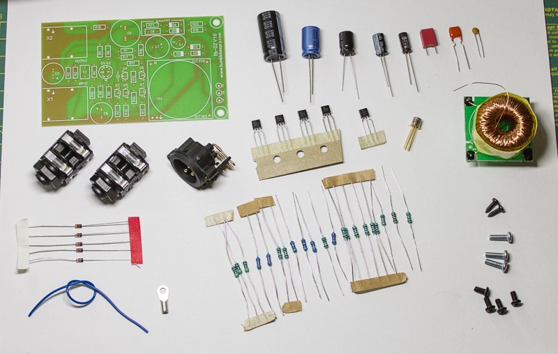
Here’s what you receive:
- All the electronic parts – resistors, capacitors, diodes
- LSK389B dual Jfet transistor
- BC547C and BC557C bipolar transistors
- Custom designed toroidal output transformer
- Neutrik connectors – a pair of jacks and an output XLR
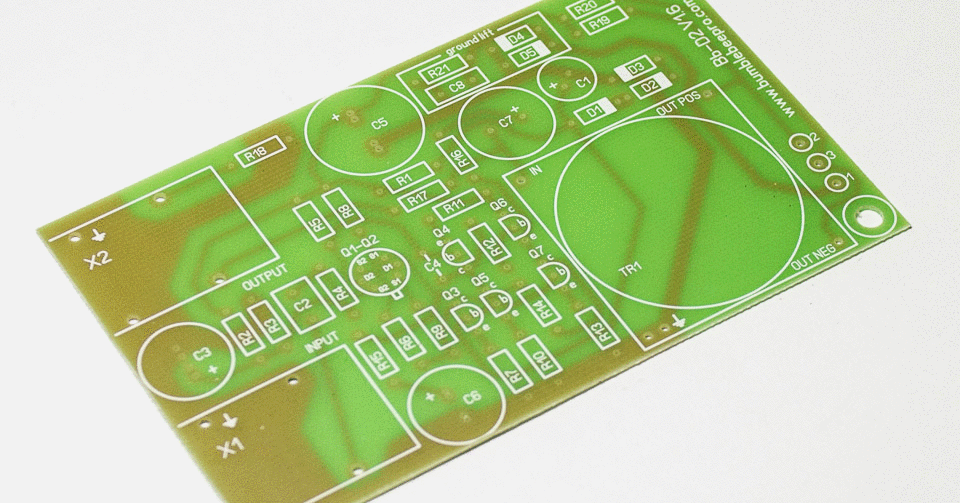
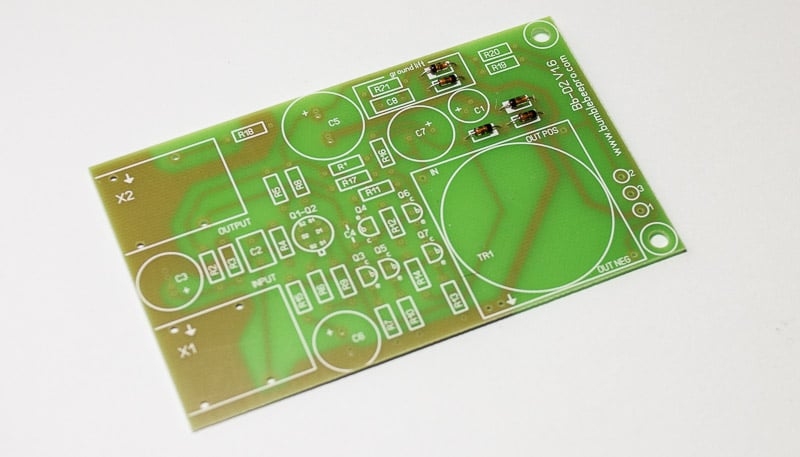
- PCB (printed circuit board)
- Wire for grounding the top of the enclosure
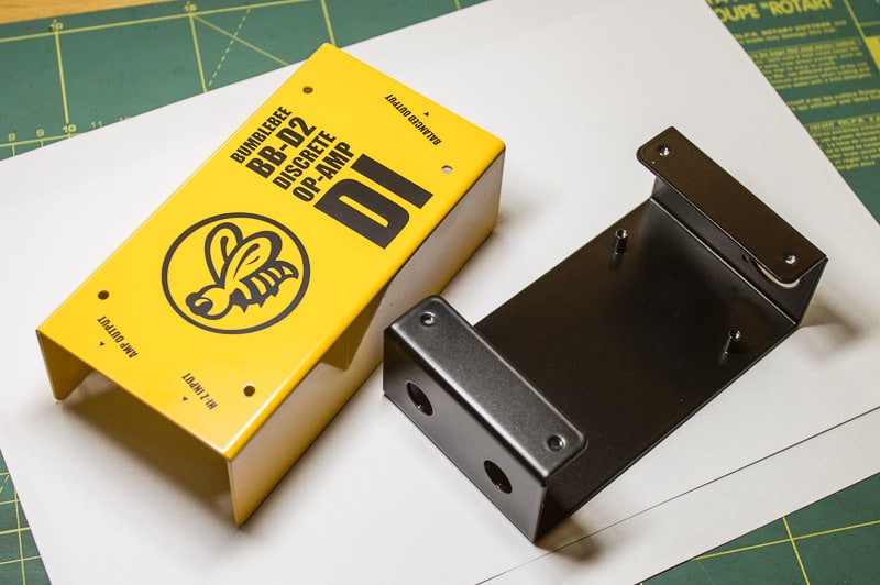
- Pre-drilled and punched, powder coated and silkscreened enclosure
- All the required screws
What else is needed:
- Soldering iron with fine tip
- Some solder wire, preferably 0.5 mm thick
- Digital multimeter for sorting the resistors
- 5/64 Hex Wrench (Allen Key) or screwdriver with 5/64 hex head.
- Philips screwdriver
- Some type of wire cutters to clip the component leads.
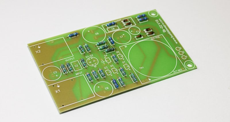
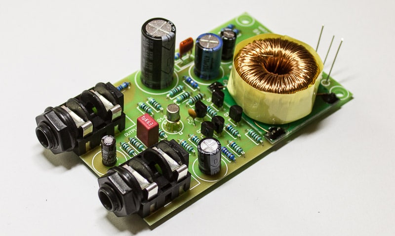
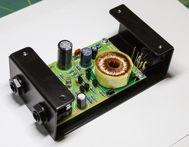
That’s how the kit looks when unpacked:
2. Solder the diodes on the PCB
So, let’s begin with assembling the PCB. I always advice to solder the smallest components first and proceed to bigger ones with each step. There are five pcs of 1N4148 diodes in the kit. Place them on their spots marked as D1, D2, D3, D4 and D5. Note that the diodes are polarized! The black band on the diode must align with the white band on PCB marking. Diodes are heat sensitive! So the best practice is to solder one lead of each diode first and then proceed to the second lead of each diode, this way you will give them some extra time to cool down.
3. Solder the resistors on the PCB
OK, this part usually takes the most of the time, as you have to measure all the values. So, get the multimeter, take a random resistor out of the bunch and measure its value. Then find the value in the list below and see where it goes on PCB. Insert it and proceed with the next one until you have all the resistors in their places. Resistors are not polarized, so don’t stress about their orientation.
- 47Ω: 2 pcs, R16 and R21
- 510Ω: 1 pc, R13
- 1.2KΩ: 1 pc, R11
- 2.7KΩ: 1 pc, R7
- 3.32KΩ: 2 pcs, R19 and R20, 0.1% precision matched
- 3.6KΩ: 6 pcs, R6, R9, R10, R12, R14 and R15
- 4.7KΩ: 3 pcs, R5, R8 and R17
- 10KΩ: 1 pc, R1
- 100KΩ: 2 pcs, R2, R3
- 1MΩ: 1 pc, R18
- 10MΩ: 1 pc, R4
Note that many digital multimeters cannot measure the value of 10MΩ, so if yours can’t, it will be the only resistor you can’t get the reading for.
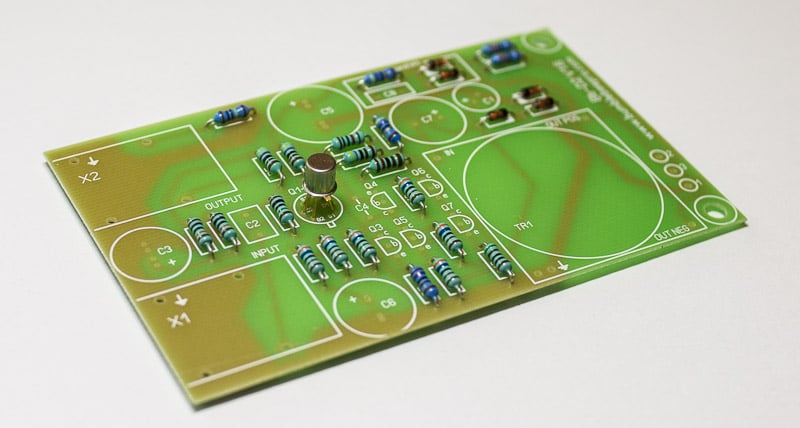
4. Solder the LSK389B dual jfet on the PCB
It is very easy to spot the LSK389B in the bunch of components – it is a metal can with six gold-plated leads. It goes to the spot on PCB marked Q1-Q2. The can has a small “dent” on the rim for proper orientation. It should be aligned with the one marked on PCB, e.g. should face down if you look at PCB from above. Insert the jfet and make sure that the leads don’t twist (sometimes it happens), so each lead goes where it should. Solder very carefully, one lead at a time and let about 10 seconds to cool down before soldering the next one. Jfet is heat-sensitive, so keep the soldering times to minimum!
5. Solder the bipolar transistors on the PCB
There are two types of bipolar transistors in this direct box circuit – BC547C (NPN) and BC557C (PNP). The part type is printed on the flat side of transistor body.
- BC547C: 4 pcs, Q3, Q5, Q6, Q7
- BC557C: 1 pc, Q4
Place the transistors on their spots. The rounded side of a transistor must align with the rounded part on PCB marking. Again, solder one lead of each transistor at a time. Transistors are heat-sensitive, so solder them quickly.
![]()
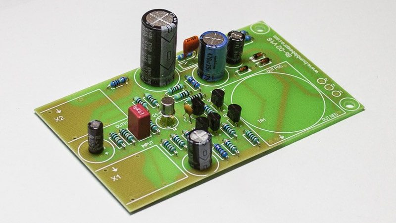
6. Solder the capacitors on the PCB
There are eight capacitors in the kit and five of them are electrolytic, which means that they are polarized! Here is the list.
Non-polarized capacitors (film and ceramic):
- 100pF: C4, the smallest one
- 47nF (typically): C8, note, the actual value of C8 can vary from 33nF to 100nF!
- 1uF: C2, the red rectangular one
Polarized capacitors (electrolytic, look like barrels):
These capacitors must be oriented properly. The positive side is marked on PCB with + sign. The negative side is marked on capacitors themselves. You can also see the photo below to check if the electrolytic capacitor orientation is correct.
- 47uF/35V: C3
- 220uF/35V: C6
- 330uF/10V: C1
- 470uF/35V: C7 (audio grade electrolytic capacitor)
- 1000uF/50V: C5
IMPORTANT NOTE: don’t throw away the leads of biggest capacitors after you clip them off, you will need them a little later!
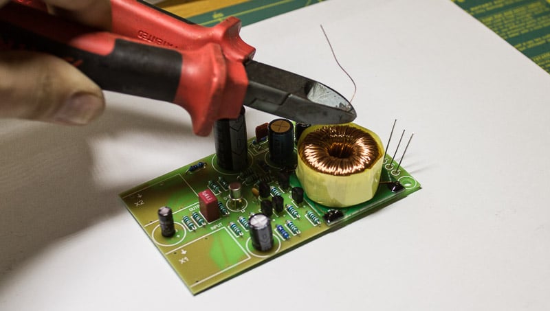
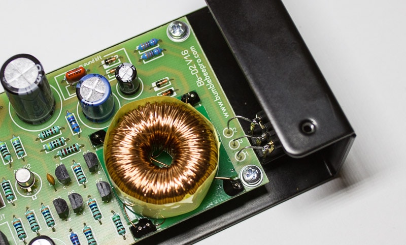
7. Solder the output transformer and output jumpers on the PCB
The transformer step is simple. Just place the transformer on PCB and solder the leads. There is one double lead for proper orientation, so there is no way to place the transformer incorrectly.
Now, regarding the jumpers. Remember, you’ve saved the leads from electrolytic capacitors? Now it is time to use them. Solder the leads into the circles marked 1, 2 and 3 next to the transformer. These jumpers will be used to connect the PCB to the output XLR.
![]()
Note that there is a flying lead on the transformer. It is normal. This lead is the end of a Faraday shield. It must not be connected anywhere. Cut it off approximately 10 mm away from the transformer body.
8. Solder the input and output jack sockets on PCB
This step is easy as well, but make sure to solder the jack sockets so they sit firmly on the surface of PCB and their leads are fully into the holes. The PCB alignment inside the enclosure depends on these sockets, so pay attention. Both sockets are of the same type.
Congrats, you are done with PCB!
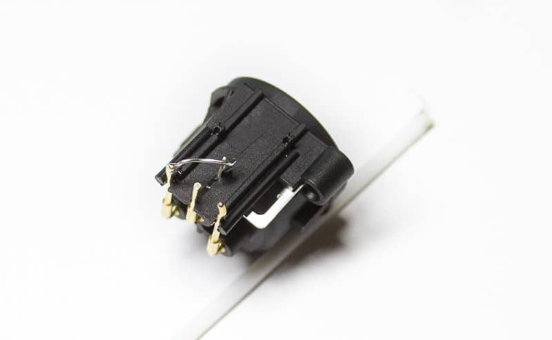
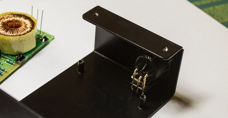
9. Fix the output XLR in the enclosure
First, you have to solder a jumper on output XLR as shown on photo below. The jumper is required to connect the bottom part of the enclosure to the cable screen/ground. Use one of the component leads you had clipped while assembling the PCB for the jumper.
Now, place the output XLR as shown on picture below and fix with two 2.6mm self-tapping screws (included in the kit). When you force them in remember the rule of thumb for any self-tapping screw – half-turn in, quarter-turn out all along the way until it is fully in.
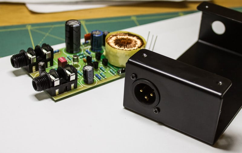
10. Fix the PCB in the enclosure
Remove the nuts and washers from jack sockets and insert the PCB into the enclosure, the socket side first. Put the washers and nuts back, but don’t fasten them tightly yet. Now use the white 8mm M3 screws (remember the washers too!) to fix the PCB in place. You might need to adjust its position slightly, so the screws would go in. When the screws are fully in, fasten the jack socket nuts tightly. I advice not to use any tools for this job, as plastic thread can be damaged if over-tighten.
11. Solder the jumpers to the output XLR
As simple as it is. Solder the jumpers to the XLR plug in the same order as they are on PCB. Note, if you prefer to go the easier way – start with the middle one!
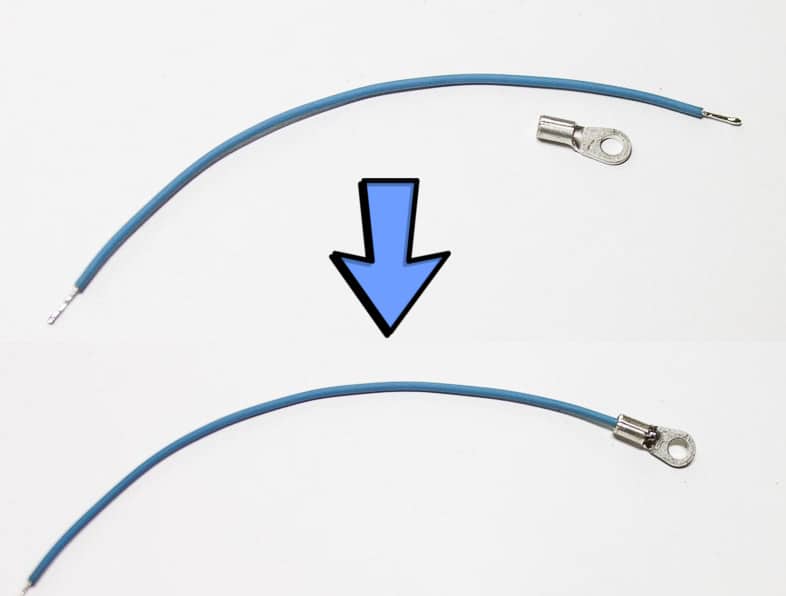
12. Solder the screw terminal on a grounding wire
Strip and tin the ends of a wire and solder the M3 screw terminal on one end.
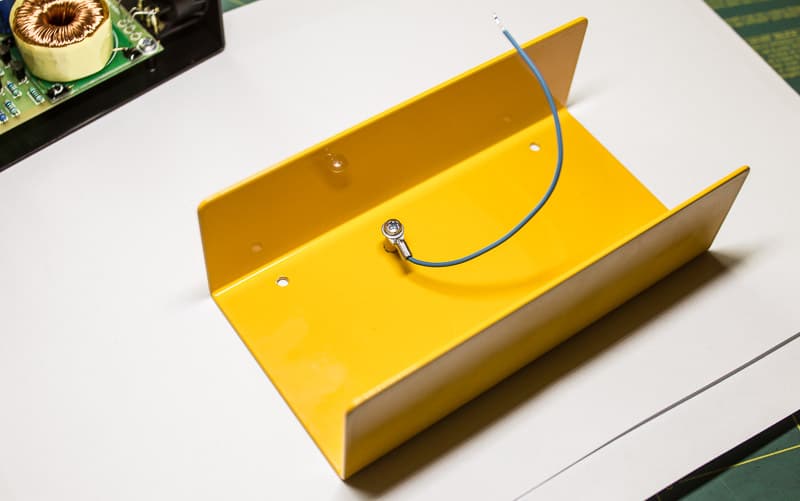
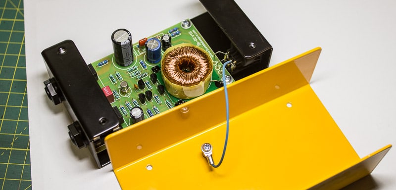
13. Attach the grounding wire to the top part of the enclosure
Use the white 8mm M3 screw with a washer to fix the grounding wire to the top of the enclosure as shown on photo below. Note, the tail of the terminal must look “down” exactly as shown below. Otherwise it might not fit well among the large components on PCB and you will have problems closing the box.
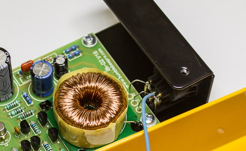
14. Solder the grounding wire to XLR
Now, solder the free end of a grounding wire to pin-1 of output XLR. Pin-1 is the closest to the side of the enclosure, it is connected with a jumper to a spot marked with “1” on PCB.
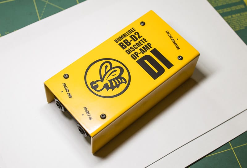
15. Close the enclosure
Well, you’ve done! Now just close the box and use the black 6mm M3 screws with hex heads to fix the enclosure parts together. Plug in your instrument, switch ON the phantom power and enjoy!
16. Test the phasing of the DI
Now, when you’ve assembled the DI, I would strongly advice to check the phasing, as sometimes the phasing of output transformers varies. It is very easy to do:
- Connect the amp out of the DI to the line input (or Hi-Z input) of a mixing/recording device, be it a console or audio interface.
- Connect the balanced out of the DI to the microphone input of the same device (and switch the phantom power on).
- Connect the instrument to the input of the DI, start picking notes and adjust the gains on both channels, so they show approximately the same input level.
- Now see the master level. If master shows nearly no signal when both inputs are active, but gets back to normal when one of two channels is deactivated, it means that the balanced output is out of phase.
So, if you have discovered that outputs of your DI are out of phase, just open the box and swap the jumpers that connect pins 2 and 3 of the XLR. It will reverse the phase back to normal. Just make sure that jumpers are not in contact when you cross them.[/vc_column_text][/vc_column][/vc_row]